3-in-1 Alternative Energy Car DIY STEM Kit
$19.99$12.95
Posted on: Apr 11, 2003

Nanowires and carbon nanotubes, each with their pluses and minuses, are advertised as the next-generation building blocks for electronic circuits a thousand times smaller than today's semiconductor circuits.
Peidong Yang, a University of California, Berkeley, chemist, has now fabricated a new type of nanotube, made of gallium nitride, that, he says, "captures some of the great properties from nanowires and carbon nanotubes, and eliminates the not-so-good characteristics of both.
"Each of these - semiconductor nanowires, carbon nanotubes and semiconductor nanotubes - will play a big role in nanocircuits of the future."
Yang, an assistant professor of chemistry at UC Berkeley and a faculty scientist at Lawrence Berkeley National Laboratory (LBNL), chemistry graduate student Joshua Goldberger and their colleagues will publish details of their synthesis in the April 10 issue of Nature.
Unlike many other inorganic nanotubes created to date, these nanotubes are perfect single crystals with interesting optical properties carbon nanotubes don't have. And because it is easy to attach organic molecules to gallium nitride surfaces, the hollow tubes hold promise as chemical sensors.
Gallium nitride also is a material well known in the semiconductor industry, and is used in many optical, high-temperature and high-voltage electronic circuits. Industry's ability to manipulate gallium nitride means that Yang's development paves the way for relatively inexpensive, large-scale production of high-quality, uniform nanotubes.
The molecular structure of a carbon nanotube is often depicted as rolled chicken wire, though, in fact, the tube is pure carbon, with dimensions on the order of 1 to 10 nanometers wide and perhaps 100 to 1,000 times that in length. By comparison, a hair is about 100,000 nanometers across. Depending on details of their synthesis, carbon nanotubes can act like conducting metals or semiconductors, and have found use in elementary transistors and chemical sensors.
The tubes have problems, however. It is difficult to make them with predictable properties, and, because they're hydrophobic, that is, they repel water, it is hard to attach organic molecules like proteins without destroying their electronic properties.
Similarly, nanowires of zinc oxide (ZnO) can be made 100 to 1,000 times longer than their width, and, as Yang proved in 2001, they can be made to emit blue through ultraviolet laser light.
Using his expertise in fabricating zinc oxide nanowires, Yang tried making nanotubes by casting gallium nitride (GaN) around nanowires and then dissolving the nanowires, in a method similar to the lost wax process employed by sculptors in bronze.
Because the crystal or lattice structures of ZnO and GaN are similar, he was able to grow pure crystalline GaN around the nanowires via chemical vapor deposition, then heat everything up to evaporate the ZnO. The precision of his technique led him to call it epitaxial casting, after epitaxy, a precise method of applying thin chemical films to semiconductors and other materials.
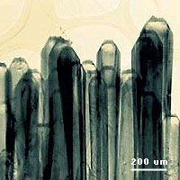
Yang's standard technique for making nanowires creates millions of them at a time in arrays that look, under an electron microscope, like the hairs of a brush. As a result, his first attempts at casting nanotubes employing nanowire templates produced a forest of hollow GaN nanotubes. Tubes can be created with inner diameters ranging from 30 to 200 nanometers and wall thicknesses ranging from 5 to 50 nanometers. Yang sees no barrier to creating GaN nanotubes as long as 20 or more microns, several hundred times their width.
Since his initial experiments, he has succeeded in growing single nanotubes, and he predicts they will have great usefulness in microfluidics to move molecules from one microscopic chamber to another. A process called nanocapillary electrophoresis could separate molecules in the same way as do today's microscale labs-on-a-chip.
"This opens up the possibility of using these very new nanotubes for nanofluidic applications," said Yang. "For example, you could use them to mimic ion channels like those in cells of the body."
Current techniques for creating nanochannels are low yield and very expensive, he said.
Because GaN nanotubes are essentially transparent, molecules also could be trapped inside and probed with various wavelengths of light.
Yang is particularly intrigued by the potential to attach molecules to the inside and/or outside of these nanotubes and use them as sensors - like little noses that, when they smell something, alter the electrical properties of the nanotube and trigger an electrical signal.
Yang also notes that his epitaxial casting technique could be used to create thin-walled nanotubes of other types of semiconducting materials.
Coauthors with Yang and Goldberger are Rongrui He and Haoquan Yan of UC Berkeley and Yanfeng Zhang, Sangkwon Lee and Heon-Jin Choi of LBNL.
The research was supported by the Camille and Henry Dreyfus Foundation, the Research Corporation, the Hellman Family Faculty Foundation. the Beckman Foundation, the National Science Foundation and the U.S. Department of Energy.
 'As far as the laws of mathematics refer to reality, they are not certain; and as far as they are certain, they do not refer to reality.'