Battery-Powered Balancing Robot DIY STEM Kit
$9.99$4.95
Posted on: Aug 24, 2006

Scientists at the Commerce Department’s National Institute of Standards and Technology (NIST) have used a beam of electrons to move a single atom in a small molecule back and forth between two positions on a crystal surface, a significant step toward learning how to build an “atomic switch” that turns electrical signals on and off in nanoscale devices.
The results, described in the Aug. 18, 2006, issue of Science,* are the first to be published about work at NIST’s new Center for Nanoscale Science and Technology.
'It’s still futuristic to talk about a real atomic switch but we’re getting closer,” says physicist Joseph Stroscio, lead author of the paper. In addition, by applying the findings to nanoscale fabrication on semiconductors and insulating thin films, it may be possible to develop new classes of electronic and magnetic devices constructed atom by atom.
In the work described in Science, NIST physicists used a custom-built, cryogenic scanning tunneling microscope (STM)—which provides a voltage and beam of electrons at its needle-like tip—to perform several different types of atomic scale measurements and manipulations. NIST theorists performed calculations of the atoms’ electronic structure, which confirmed the experimental results.
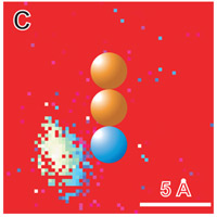
A molecular chain of one cobalt atom and several copper atoms set upon a surface of copper atoms was constructed atom by atom using the STM in an atom manipulation mode. Then the STM was used to shoot electrons at the molecular chain and its effect on the switching motion of the cobalt atom was measured.
In addition, the team used a “tunneling noise spectroscopy” technique to determine how long the atom stays in one place. This measurement method was developed by two of the authors based on their 2004 discovery that an atom emits a characteristic scratching sound when an STM is used to move the atom between two types of bonding sites on a crystal**
“The two most important new findings,” Stroscio says, “are an increased understanding of the science behind atomic switching and the development of a new measurement capability to spatially map the probability of an electron exciting the desired atom motion.”
The scientists analyzed what happened to the atom switching rate as changes occurred in the STM voltage and in the current between the STM tip and surface. Above a threshold voltage of about 15-20 millivolts, the probability for switching per electron is constant, meaning that the electrons contain sufficient energy to move the cobalt atom. Higher currents result in faster switching.
The data suggested that a single electron boosts the molecule above a critical energy level, allowing a key bond to break so the cobalt atom can switch positions. The cobalt atom was less likely to switch as the molecular chain was extended in length from two to five copper atoms, demonstrating that the atom switching dynamics can be tuned through changes in the molecular architecture.
The researchers also found that the position of the STM tip is critical. They made this discovery by recording detailed noise measurements of the molecule with atomic scale resolution. An analysis of the noise enabled the team to make a spatial map of the switching speed and probability, showing that switching is most likely when the STM tip is positioned to the left of the cobalt atom. This finding is consistent with calculations of electronic structure and demonstrates the need to inject energy into a particular bond, according to the paper.
“This insight raises the possibility that molecular orbital analysis may be used to guide the design and control of single atom manipulation in nanostructures,” the authors write.
The work was supported in part by the Office of Naval Research.
As a non-regulatory agency of the U.S. Department of Commerce’s Technology Administration, NIST promotes U.S. innovation and industrial competitiveness by advancing measurement science, standards and technology in ways that enhance economic security and improve our quality of life.
*J.A. Stroscio, F. Tavazza, J.N. Crain, R.J. Celotta, and Anne M. Chaka. Electronically Induced Atom Motion in Engineered CoCun Nanostructures. Science. Aug. 18, 2006.
**J.A. Stroscio and R.J. Celotta. Controlling the Dynamics of a Single Atom in Lateral Atom Manipulation. Science Express, Sept. 9, 2004.
 'Physicists like to think that all you have to do is say, these are the conditions, now what happens next?'