Simple DC Motor DIY STEM Kit
$9.99$4.95
Posted on: Nov 13, 2006

A new form of scanning microscopy that simultaneously reveals physical and electronic profiles of metal nanostructures has been demonstrated at JILA, a joint institute of the National Institute of Standards and Technology (NIST) and University of Colorado at Boulder. The new instrument is expected to be particularly useful for analyzing the make-up and properties of nanoscale electronics and nanoparticles.
Scanning photoionization microscopy (SPIM), described in a new paper,* combines the high spatial resolution of optical microscopy with the high sensitivity to subtle electrical activity made possible by detecting the low-energy electrons emitted by a material as it is illuminated with laser pulses. The technique potentially could be used to make pictures of both electronic and physical patterns in devices such as nanostructured transistors or electrode sensors, or to identify chemicals or even elements in such structures.
“You make images by virtue of how readily electrons are photoejected from a material,” says NIST Fellow David Nesbitt, leader of the research group. “The method is in its infancy, but nevertheless it really does have the power to provide a new set of eyes for looking at nanostructured metals and semiconductors.”
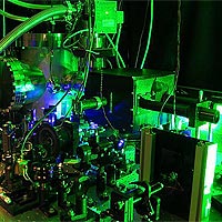
The JILA-built apparatus includes a moving optical microscopy stage in a vacuum, an ultrafast near-ultraviolet laser beam that provides sufficient peak power to inject two photons (particles of light) into a metal at virtually the same time, and equipment for measuring the numbers and energy of electrons ejected from the material. By comparing SPIM images of nanostructured gold films to scans using atomic force microscopy, which profiles surface topology, the researchers confirmed the correlations and physical mapping accuracy of the new technique. They also determined that lines in SPIM images correspond to spikes in electron energy, or current, and that contrast depends on the depth of electrons escaping from the metal as well as variations in material thickness.
Work is continuing to further develop the method, which may be able to make chemically specific images, for example, if the lasers are tuned to different colors to affect only one type of molecule at a time. The research is supported by the Air Force Office of Scientific Research and National Science Foundation.
* O.L.A. Monti, T.A. Baker and D.J. Nesbitt. 2006. Imaging nanostructures with scanning photoionization microscopy. Journal of Chemical Physics, October 21.
 'We should take care not to make intellect our god; it has powerful muscles but no personality.'