3-in-1 Alternative Energy Car DIY STEM Kit
$19.99$12.95
Posted on: Jul 14, 2007

Around the world, students learn about the wave nature of light through the interference patterns of “Young’s double-slit experiment,” first performed more than 200 years ago and still considered among the most beautiful physics experiments. Using an analogous experiment, researchers at Brown and Stanford have shown that a simple analytical model can describe the wave nature of surface plasmon polaritons. Their work suggests that plasmonic devices cannot easily circumvent the limitations of electromagnetic waves.
In an experiment modeled on the classic “Young’s double slit experiment” and published in the journal Nature Nanotechnology, researchers have powerfully reinforced the understanding that surface plasmon polaritons (SPPs) propagate and diffract just like any other wave. The demonstration reminds researchers and electronics designers that although SPPs move along a metal surface, rather than inside a wire or an optical fiber, they cannot magically overcome the size limitations of conventional optics.
Image
Touted as the next wave of electronics miniaturization, plasmonics describes the movement of SPPs – a type of electromagnetic wave that is bound to a metal surface by its interaction with surface electrons. The emerging technology could provide a bridge between nanoscale electronics and photonics. Conventional electronic devices, in which metal wires carry electrical signals, can be manufactured at the nanoscale but incur long time delays. Photonic – or fiber optic – devices transmit a signal at the speed of light but cannot be miniaturized below a size limit imposed by the wavelength of light that they carry.
Plasmonic devices seem to combine the best of both technologies. Because SPPs are electromagnetic waves they move at near light-speed, but because they ride the surface of wires, it seemed they might circumvent the diffraction limit, which restricts the size of fiber optics.
“We know that these are still essentially electromagnetic waves and therefore they must still obey a diffraction limit,” says Rashid Zia, assistant professor of engineering at Brown University. “The key is to define a set of solutions in a way that is analogous to other systems so that we can derive that limit.”
Zia and Mark Brongersma, an assistant professor of engineering at Stanford University, set out to find an experiment that could test the limits of plasmonic technology and also shed light on the principles that control this still-mysterious kind of wave.
Young’s double slit experiment is usually performed as a demonstration of optical diffraction, although recent variations have also been used to test the quantum behavior of electrons, atoms and even molecules.
In the classic double slit experiment, students shine a light onto a screen through an opaque barrier with two slits in it. When one slit is covered, the pattern of light is brightest directly in front of the slit. When light passes through both slits, a series of light and dark lines appear instead. The light forms a bright line between the slits, where the peaks of the waves reinforce one another and a distinct pattern of darker lines where the peaks and valleys cancel each other out. It’s an elegant demonstration of the wave side of light’s dual nature.
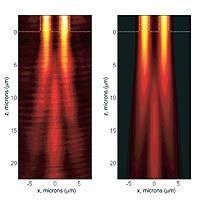
In their experiment, Zia and Brongersma generated an SPP and passed it across two narrow bridges of gold film on a glass slide. As the waves exited onto a broad sheet of gold film, they diffracted to create interference patterns analogous to those seen in Young’s double slit experiment. Using a simple analytical model for the way SPPs are guided along individual metal stripes, the researchers predicted the pattern of diffraction they would see.
Because SPPs are not in the spectrum of visible light, they don’t just show up on a screen. Zia and Brongersma precisely measured the diffraction pattern using a photon scanning tunneling microscope. The pattern they saw closely matched what they predicted using their proposed framework, which is based on an analogy to conventional optics.
The results of this experiment may disappoint some researchers who have hoped that SPPs traveling along metal waveguides could allow circuit design to move seamlessly from electronics to photonics. Instead, Zia sees developing – and challenging – a comprehensive theory as the first step toward devising structures uniquely suited to controlling the movement of SPPs.
“You can couple stripes, you can make slits, you can make all sorts of other geometries that might work,“ said Zia. ”But to see that potential through, you have to have a clear analytical theory and a way to test it.”
 'There must be no barriers for freedom of inquiry. There is no place for dogma in science. The scientist is free, and must be free to ask any question, to doubt any assertion, to seek for any evidence, to correct any errors.'