Battery-Powered Balancing Robot DIY STEM Kit
$9.99$4.95
Posted on: Oct 30, 2011

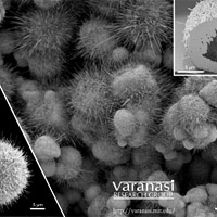
Images taken with a Field Emission Scanning Electron Microscope show the nanowire bristles that form on copper particles of different sizes. At top right, a cross-section of one of the particles reveals its hollow interior.
Images courtesy of the Varanasi Lab
Sometimes, a simple decision to try something unconventional can lead to a significant discovery.
A well-known method of making heat sinks for electronic devices is a process called sintering, in which powdered metal is formed into a desired shape and then heated in a vacuum to bind the particles together. But in a recent experiment, some students tried sintering copper particles in air and got a big surprise.
Instead of the expected solid metal shape, what they found was a mass of particles that had grown long whiskers of oxidized copper. “It was sort of serendipitous,” says Kripa Varanasi, d’Arbeloff Assistant Professor of Mechanical Engineering at MIT. “We got this crazy stuff, particles covered in nanowires,” he says.
The resulting process could turn out to be an important new method for manufacturing structures that span a range of sizes down to a few nanometers (billionths of a meter) in size. “You go in one step from solid spherical powder to very complex structures,” says Christopher Love, a mechanical engineering graduate student who is lead author on the paper. “The process is very simple, and the structures are durable,” he says. These new structures could be used for managing the flow of heat in various applications ranging from powerplants to the cooling of electronics.
Not only were the particles covered with fine wires, but the abundance of the wires turned out to be dependent on the size of the original copper particles. “We are the first to observe a size-dependent oxidation in copper,” Varanasi says. That means researchers can easily synthesize porous structures at various scales, in bulk, by selecting the particles they start out with: Particles smaller than a certain size sinter, while larger particles grow nanowires.
The discovery is reported in a paper being published in the journal RSC Nanoscale. In addition to Varanasi and Love, the paper’s authors are mechanical engineering graduate student J. David Smith and postdoc Yuehua Cui of the Laboratory for Manufacturing and Productivity.
Such hierarchical structures can be very effective for thermal management, cooling everything from microprocessors to the boilers of huge powerplants. They might even prove useful in engineered geothermal power, which holds great promise as a system for providing clean, renewable power. Because the resulting structures are so easily controlled, “you can optimize them to control phenomena taking place at different length and time scales,” Varanasi says.
While the growth of nanowires on bulk copper sheets had been observed before, Varanasi says, this is the first time it has been observed across a variety of size scales at once, and the first time the process has been analyzed and explained. “There have been a bunch of different theories about how these nanowires grow,” he says. But now, “this paper established thoroughly” what the mechanism is for copper particles: The bristles grow outward through diffusion, leaving the particles hollow in the middle as the metal migrates outward.
The team is now testing the same process with other materials. For example, if it works with zirconium — the metal now used as the cladding for fuel rods in nuclear reactors — it might help improve heat transfer. In a nuclear reactor, where this process drives turbines and produces power, such an advance could boost the reactors’ overall efficiency.
In addition to thermal management, these results could help to optimize certain catalytic processes, Varanasi says.
Suresh Garimella, a professor of mechanical engineering at Purdue University who was not involved in this research, says the “simple and potentially cost-effective nature of the method” for growing copper nanowires “makes the findings significant,” with potential applications including catalysis and thermal management.
Brent Segal, chief technologist at Lockheed Martin Nanosystems in Billerica, Mass., says this is “significant work on controlling the electrical properties and thermal properties” of materials, and possibly their optical properties as well. Such control, from the microscopic to the nanoscopic scale — a thousand-fold difference in size — “has not been seen before” in a single process, he says.
Upon seeing the team’s description of this new technique, Segal says, “You immediately think, ‘I want to go try 75 other materials’” to see if they work in a similar way. “I think 100 different labs around the country will try everything they’ve got on the shelf” using this technique, he adds.
The work was supported by the MIT Deshpande Center, a DARPA Young Faculty Award, the MIT Energy Initiative, and a National Science Foundation graduate research fellowship.