Solar + Battery Car DIY STEM Kit
$11.99$5.95
Posted on: Jul 16, 2011

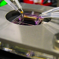
Zinc oxide nanostructures are directly synthesized in parallel microfluidic channels (held by the metal frame) by flowing reactants through the tubing. The microfluidic structure not only creates the device, but also becomes the final packaged functional LED device itself.
Photo: Jaebum Joo
Researchers at MIT have found a way to grow submicroscopic wires in water with great precision, using a method that makes it possible to produce entire electronic devices through a liquid-based process.
The team demonstrated the technique, called hydrothermal synthesis, by producing a functional light-emitting diode (LED) array made of zinc oxide nanowires in a microfluidic channel. They were able to do so on a lab bench under relatively benign conditions: essentially using a syringe to push solution through a capillary tube one-tenth of a millimeter wide, without expensive semiconductor manufacturing processes and facilities.
Unlike larger structures, with nanomaterials — those with dimensions measured in nanometers, or billionths of a meter — differences in shape can lead to dramatic differences in behavior. “For nanostructures, there’s a coupling between the geometry and the electrical and optical properties,” explains Brian Chow PhD ’08, co-author of a paper describing the results that was published July 10 in the journal Nature Materials. “Being able to rationally tune the geometry is very powerful because you can, in turn, tune the functional properties.” The system Chow and his colleagues developed can precisely control the aspect ratio (the ratio of length to width) of the nanowires to produce anything from flat plates to long, thin wires.
There are other ways of making such nanowires, says Chow, who did this work as a postdoc at MIT. “People have demonstrated good control over the morphology of wires by other means, particularly at much higher temperatures or in organic solvents. But to be able to do this in water under these low-temperature conditions is attractive” because it may make it easier to manufacture such devices on flexible polymers and plastics, he says.
Control over the shapes of the wires has until now been largely a trial-and-error process. “We were trying to find out what is the controlling factor,” explains Jaebum Joo PhD ’10, now a senior research scientist at Dow Chemical Co., who was the lead author of the paper.
The key turns out to be the electrostatic properties of the zinc oxide material as it grows from a solution, they found. The ions of different compounds, when added to the solution, attach themselves electrostatically only to certain parts of the wire — just to the sides, or just to the ends — inhibiting the wire’s growth in those directions. The amount of inhibition depends on the specific properties of the added compounds.
While this work was done with zinc oxide nanowires — a promising material that is being widely studied by researchers — the MIT scientists believe the method they developed for controlling the shape of the wires “can be expanded to different material systems,” Joo says, perhaps including titanium dioxide, which is being investigated for devices such as solar cells. Because the benign assembly conditions allow the material to be grown on plastic surfaces, he says, it might enable the development of flexible display panels, for example.
But there are also many potential applications using the zinc oxide material itself, including the production of batteries, sensors and optical devices. And the processing method has “the potential for large-scale manufacturing,” Joo says.
The team also hopes to be able to use the method to make “spatially complex devices from the bottom up, out of biocompatible polymers,” Joo adds. These could be used, for example, to make tiny devices that could be implanted in the brain to provide high-resolution, long-term sensing and stimulation.
Manu Prakash PhD ’08, now an assistant professor of bioengineering at Stanford University, says this was a very interdisciplinary project that emerged when he (studying applied physics), Joo (studying nanomaterials) and Chow (in applied chemistry) were close friends in graduate school and began discussing better ways to manufacture electronic circuits. “We began talking about how our different fields affected this one problem,” Prakash says.
They talked about the inefficiency of present methods, where electronic circuits are first built, then packaged, and finally tested. They realized, he says, that “all these things could be done in one shot,” and that’s what they were able to demonstrate in the work described in this paper: The microfluidic device used for processing became the final packaging of the device, and testing was carried out continuously through the manufacturing process. “It’s a bottom-up way of thinking about it,” Prakash says. “The packaging is part of the way they’re synthesized.”
Christopher Murray, University Professor of Chemistry and Materials Science and Engineering at the University of Pennsylvania, calls this paper a “valuable contribution.” Murray, who was not involved in this research, adds: “We are seeing a convergence right now, and it will really change our understanding of nanomaterials synthesis and systems integration.” This paper, he says, is “a very nice piece of work.”
The research was carried out with Media Lab associate professors Edward Boyden and Joseph Jacobson, and was funded by the MIT Center for Bits and Atoms, the MIT Media Lab, the Korea Foundation for Advanced Studies, Samsung Electronics, the Harvard Society of Fellows, the Wallace H. Coulter Early Career Award, the NARSAD Young Investigator Award, the National Science Foundation and the NIH Director’s New Innovator Award.
 'There comes a time when the mind takes a higher plane of knowledge but can never prove how it got there. All great discoveries have involved such a leap. The important thing is not to stop questioning.'